- You are here:
- Knowledge »
- Blog »
- Welcome
Welcome
- 24. September 2018
In the future our blog will regularly inform you about the latest developments in the areas of Electronic Design Automation (EDA) as well as the complete digitalisation of business processes.
The digital future is here already. Cloud Computing, Internet of Things, Industry 4.0 and Autonomous Driving are already part of everyday business.
Nearly every day we hear about new developments and progress in the fields of FPGA design, PCB design and wiring harness design. Progress only spoken about yesterday has become reality today. The necessity for Lifecycle Management Systems for new products (PLM) and application development (ALM) is more important than ever before.
Together with international industry experts we will regularly bring you constructive suggestions, news and technical information. Let us inspire you with our vision for the digital world to become a reality.
Your TRIAS Team
Requirement Driven HW Design and Verification
Free download of English presentation
Team based requirement driven HW design and verification enable efficient design and verification process through focusing on:
What is needed (Requirements)
What should be done (Implementation)
Does it works (Verification)
This presentation will give an overview of different methods to integrate the requirement management platform Polarion ALM to streamline SoC verification with Questa.

By loading the video, you agree to Vimeos's privacy policy.
Learn more

By loading the video, you agree to Vimeos's privacy policy.
Learn more

By loading the video, you agree to Vimeos's privacy policy.
Learn more

By loading the video, you agree to YouTube's privacy policy.
Learn more

By loading the video, you agree to YouTube's privacy policy.
Learn more

By loading the video, you agree to YouTube's privacy policy.
Learn more

By loading the video, you agree to YouTube's privacy policy.
Learn more

By loading the video, you agree to YouTube's privacy policy.
Learn more

By loading the video, you agree to YouTube's privacy policy.
Learn more

By loading the video, you agree to Vimeos's privacy policy.
Learn more

By loading the video, you agree to Vimeos's privacy policy.
Learn more

By loading the video, you agree to Vimeos's privacy policy.
Learn more

By loading the video, you agree to Vimeos's privacy policy.
Learn more

By loading the video, you agree to Vimeos's privacy policy.
Learn more

By loading the video, you agree to Vimeos's privacy policy.
Learn more
Functional correctness of FPGA synthesis from RTL code to final netlist
Systematic design errors, introduced by automated design refinement tools, such as synthesis, can be hard to detect, and damaging if they make it into the final device. Formal equivalence checking has been used for ASIC design flows for many years. As FPGAs become bigger and critical system components, exhaustively verifying the functional equivalence of Register Transfer Level (RTL) code to synthesized netlists and the final placed & routed FPGA designs is mandatory.
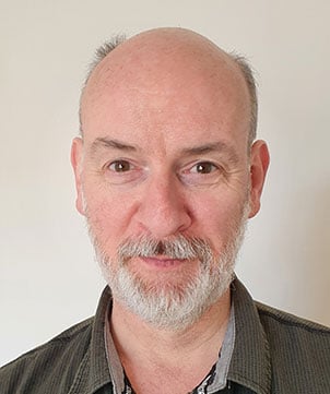 Speaker: Neil Rattray, OneSpin: A Siemens Business
Neil Rattray is Senior Field Application Engineer at OneSpin: A Siemens Business and has over 20 years of experience in EDA, supporting both design and verification flows. Neil joined the OneSpin team in 2016 and works closely with key customers.
Neil has deep technical knowledge from working as both a designer and field application engineer. He started his career as a hardware design engineer but later moved to application engineering, supporting FPGA products, before ultimately making the leap to EDA. Neil’s breadth of experience enables him to apply formal verification efficiently and thoughtfully within his customers’ design teams. He cultivates strong relationships with OneSpin 360™ users and has a passion for driving their success with the superior level of support he provides.
Neil holds a Bachelor of Engineering degree in Electronic Engineering from Queen Mary College, University of London. When not working with customers, he devotes his time to family, sports, and his many woodworking projects. He is based in the Netherlands.
VHDL testbench Randomisation – Great for better Quality
Randomization is very useful, but also very important for modern testbenches. Unfortunately, designers do not use it enough.
This presentation will show how simple it is to apply randomisation in an efficient way using the new Enhanced and Optimised Randomisation in UVVM.
As for UVVM in general, this new functionality is also free and open-source, and the readability of the syntax is really unique
 Speaker: Espen Tallaksen, EmLogic AS
Espen Tallaksen CEO, Co-founder and Principal FPGA designer at EmLogic, the new and rapidly growing Norwegian Embedded Systems & FPGA Design Centre. He has more than 30 years international experience of FPGA and ASIC development and verification, for example through work at Philips Semiconductors (NXP) in Zürich (Switzerland).
His main focus during the past 20 years has been methodology, efficiency and quality improvement for FPGA and ASIC projects, which resulted in the UVVM verification platform, which is now used worldwide. Espen is well known through his tutorials and talks, for example at FPGA Conference Europe in Germany.
What Formal Verification is about
With FPGA technology evolving rapidly, more and more functionality is being implemented in FPGAs, increasing the complexity of FPGA designs. More functionality also means it becomes harder and harder, to verify this functionality in the limited time available in the design and verification process.
With traditional verification approaches based on simulation a complete verification of such systems is hard to achieve, since there is never enough time to simulate everything possible. Formal approaches that can help find more bugs, that are likely of being missed in the design with simulation, have been available for many years.
This presentation gives an introduction as to formal verification, what different types of formal verification exist and what they do. The limitations of verification by simulation and by formal approach will be discussed.
Many problems can be found with automatic formal checks and as an example for an automatic formal solution, Questa Formal Autocheck will be introduced. It will be shown what kind of problems can be found in a design, without the need for knowledge about property descriptions, and how this can be added to the overall verification flow
 Speaker: Hans-Jürgen Schwender, TRIAS mikrolektronik
Hans-Jürgen Schwender has a masters degree in electrical engineering. From 1991 until the end of 2001, he worked as an ASIC design engineer at Philips Kommunikationsindustrie and Lucent Technologies in Nuremberg and at Infineon Technologies in San Jose, CA, USA. He worked on the creation of specifications, the implementation in VHDL, verification on module and chip level as well as programming of ASIC Driver Software in C.
Mr. Schwender has been working at TRIAS Mikroelektronik since 2002 and, as the technical manager covers a large part of Siemens EDA’s products – with a focus on HDL design, verification and cable harness design products.
Python, the alternative to your HDL testbench
Constrained randomization and functional coverage have recently become crucial elements for successful verification of FPGA and ASIC design.
SystemVerilog and UVM framework is the de-facto standard for verification. Still, due to a high learning time/benefit ratio, many users preferred to look into other alternatives such as UVVM/OSVM.
Lately, Python has emerged as a third option, and it is gaining interest for its obvious advantages (easy language, big community, extensive library …)
The purpose of this presentation is to show you how we can build a high-quality reusable verification environment using Python Libraries/Framework.
 Speaker: Faïçal Chtourou, Siemens EDA
Faïçal Chtourou is a European application engineer at Siemens EDA, specialized in Digital functional verification tools and methodology. His background includes 10+ years of experience verifying complex SOC in various markets (HPC, Automotive, Flash memory ); he has a strong interest in flow automation and RTL quality improvement.
Faïçal holds an MS degree in Microelectronics and Telecommunication from Polytech Marseille, France
Efinix® Titanium – The Low Power FPGA with a growing Feature Set
Efinix’ first FPGA family Trion is in full production and well received in the markets worldwide. Trion ranges from very small, very low power densities to low power, mid-range FPGAs. Some density devices offer hardened IP for common requirements such as MIPI CSI-2 Controllers and DDR3 Memory Controller. The latest Efinix FPGA family, Titanium, is fabricated on a 16 nm process, delivering low power, high performance and small physical size. Like Trion the Titanium Family also adds more hardened features delivering increased functionality and performance in the higher density family members.
The presentation will quickly go over the history of Efinix, the basic philosophy and differentiation. We will cover Titanium’s hardware architecture and how it combines Soft- and Hard-IP to address a wide range of applications. The feature sets of Titanium family members will be covered along with their target markets. Finally, we will cover the latest news from the Titanium family and available hard and soft IP as well as tools and software.
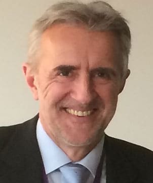 Speaker: Joachim Müller, Efinix Inc
Upon graduating at TU Braunschweig in 1989, Joachim Müller held positions in ASIC development, sales and marketing, before joining Lattice Semiconductor in October 2000 as Senior FAE. Since October 2021 he is in charge of Field Application, Europe, for Efinix Inc.
UVVM – Brand new features from the world’s #1 VHDL Verification Methodology
A good verification methodology could significantly reduce FPGA and ASIC development time. UVVM is making this much easier through the provided Testbench Infrastructure, the architecture, the BFMs and the VVCs. This presentation will briefly mention these benefits but will focus on brand new functionality to be released very soon.
This functionality is being developed in the current ESA UVVM project and has so far not been mentioned in any previous UVVM presentation.
 Speaker: Espen Tallaksen– EmLogic AS
Espen Tallaksen CEO, Co-founder and Principal FPGA designer at EmLogic, the new and rapidly growing Norwegian Embedded Systems & FPGA Design Centre. He has more than 30 years international experience of FPGA and ASIC development and verification, for example through work at Philips Semiconductors (NXP) in Zürich (Switzerland).
His main focus during the past 20 years has been methodology, efficiency and quality improvement for FPGA and ASIC projects, which resulted in the UVVM verification platform, which is now used worldwide. Espen is well known through his tutorials and talks, for example at FPGA Conference Europe in Germany.
Functional FPGA design verification by using real input data as simulation stimulus in ModelSim
For functional verification of FPGA designs, it is preferred to use a generator to produce stimulus input data. This data is fed into the simulation of the design to verify its behavior according to the underlying specification.
A difficulty in this process, which should not be underestimated, can be the development of a model for a sufficient stimulus generator to achieve an acceptable level of verification. This quickly leads to complicated model-based versions with sophisticated random models.
To address this difficulty, this talk discusses the use of a previously collected dataset of real input data to avoid a stimulus generator. How this approach can be implemented in ModelSim in an appropriate way and which effort has to be taken into account is shown by a concrete application example from signal processing with SuperSampleRate-IIR filters (digital filters, which process more than one sample per clock cycle).
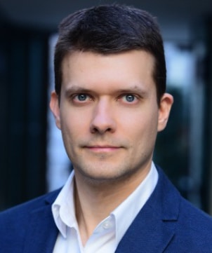 Speaker: Dr. Markus Jäger, SciCaTec
Dr. Markus Jäger is System Architect for embedded and electronic systems. His special fields are the digital circuitry and algorithmic in FPGAs, SoCs and GPUs for Signal, Video, Image Processing and Computer Vision applications. In this function and as a developer for FPGA SoC designs and embedded software, he is involved in the international development of innovative electronic systems for industry and science.
As founder of the company SciCaTec he is working as System Architect and FPGA SoC developer in high-performance Signal, Video and Image Processing in the automotive as well as industrial area. The focus is thereby on the development and implementation of specific algorithms in FPGA SoC technology.
FPGAs and Cloud – Two Sides of the Same Coin
According to Forrester Research, more than 60% of today’s cloud-users did not meet goals for both migration- and run-costs on their cloud-based deployment.
For your consideration: the development of High-Performance Computing and Verification Server farm data centers have unintentionally followed the development of FPGA architectures. Real benefits from cloud-based workflows are only available if we apply lessons learned and practiced by FPGA teams who already understand how to exploit complex heterogeneous computing architectures.
On-premises datacenters cannot provide the distinct unique configurations at scale that cloud-based verification workflows can offer within their huge variety of compute servers, memory, IO, storage, and services choices. We’ll see how realizing those advantages requires the same mindset of today’s complex FPGA project teams to define and implement the Goldilocks zone configuration for each cloud-based workflow to minimize high cloud costs and to maximize productivity.
 Speaker: David Lidrbauch, Siemens EDA (früher Mentor Graphics)
David Lidrbauch earned his Bachelor of Science in Electrical Engineering and Applied Physics at Case Western Reserve University. He began his career as a hardware design engineer pushing new technology for high-speed data interfaces and high-reliability industrial communications. As Solutions Manager for Digital Verification Technology at Siemens EDA, David uses his decades of experience in design and verification hardware and software for ASIC, FPGA, and DSP solutions to drive new verification workflows. In rare spare hours, Dave keeps old stick-shift Saabs road-worthy and is restoring an old sailboat for long-distance cruising.
Why is CDC Verification for FPGA Designs important
FPGA Designs have become very complex today, most FPGA Designs could be considered System On Chip Designs because they contain multiple complex system components with different protocol interfaces like AMBA, PCIe, Ethernet, USB, just to name a few of the most popular ones. The complexity itself is already a challenge for verification in a fully synchronous design. But the multitude of interfaces in today’s applications implies multiple, asynchronous clock domains. There are well known techniques how to get data safely from one clock domain to the other. But how can verification show that the clock domain crossings (CDC) have been designed such that data can cross them unchanged? This question needs to be answered especially in safety critical application as regular verification by simulation can’t show this.
 Speaker: Hans-Jürgen Schwender, TRIAS mikrolektronik
has a masters degree in electrical engineering. From 1991 until the end of 2001, he worked as an ASIC design engineer at Philips Kommunikationsindustrie and Lucent Technologies in Nuremberg and at Infineon Technologies in San Jose, CA, USA. He worked on the creation of specifications, the implementation in VHDL, verification on module and chip level as well as programming of ASIC Driver Software in C.
Mr. Schwender has been working at TRIAS Mikroelektronik since 2002 and, as the technical manager covers a large part of Siemens EDA’s products – with a focus on HDL design, verification and cable harness design products.
What’s next for the Lattice Nexus platform
In 2019, Lattice Semiconductor revolutionized the FPGA industry with introduction of it Lattice Nexus™ platform. The first platform developed using the company’s platform-based design approach, Nexus combines Lattice engineering advancements with 28nm FD-SOI technology to deliver class-leading low power consumption, reliability, system bandwidth, and small form factor for small, low power FPGAs. Since then, the company has delivered three FPGA device families based on the Nexus platform – CrossLink-NX for embedded vision and processing, Certus-NX for a wide array of applications, and Mach-NX for next generation, cyber-resilient systems.
In this presentation, we’ll discuss what’s next for the Lattice Nexus platform.
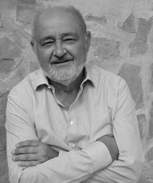 Speaker: Eugen Krassin, LEC2
Eugen Krassin immigrated to the Federal Republic of Germany at the age of 12. After graduating from secondary school, the second course of education and the subsequent Abitur, he studied Technical Informatics at the University of Stuttgart. After graduation, he worked as an ASIC developer at an avionics and guidance company before working as a freelance consultant for the development and use of FPGAs. In 1995 he and his wife founded the engineering firm PLC2, which in the following years was to become the nucleus of the PLC2 Group. In 2017 he handed over the overall responsibility of the PLC2 group to his successors. In 2018 he founded Krassin Consulting GmbH, which focuses on the establishment of a Lattice training center.
FPGA Verification Trends, Challenges, and Solutions
This presentation discusses the latest Field-Programmable Gate Array (FPGA) functional verification trends based on the recently completed 2020 Wilson Research Group industry study. The findings from this world-wide study provide invaluable insight into the state of today’s FPGA market in terms of both design and verification trends. To address the challenges identified in this study, a variety of easy to adopt advanced verification solutions will be presented, and a practical roadmap provided on how to mature your project’s verification maturity.
 Speaker: Harry Foster
is Chief Scientist Verification for the Design Verification Technology Division of Siemens EDA, A Siemens Business; and is the Co-Founder and Executive Editor for the Verification Academy. He holds multiple patents in verification and has co-authored six books on verification. Harry was the 2006 recipient of the Accellera Technical Excellence Award for his contributions to developing industry standards, and was the original creator of the Accellera Open Verification Library (OVL) standard.
 Speaker: Stefan Bauer
is Application Engineer at Siemens EDA to support the European Distribution Channel in the digital design and verification area.
Before he joined Siemens EDA in 2014, he worked as a Verification Engineer at Ericsson and ST-Ericsson in Nuremberg where he verified components of an ASIC by using SystemVerilog OVM/UVM environments, Assertions and Code Coverage.
During his job as a working student and during his master thesis at Siemens Healthcare in Erlangen, he gathered his first experiences in the FPGA area.
FPGA development meets IEC 62304 – How to optimize and automate software lifecycle processes for FPGA based medical devices.
IEC 62304 is the applicable standard, which defines the life cycle of software-based medical devices. Within this standard programmable hardware components such as FPGAs are in a grey area, as they have to be developed like any other software, but in actual use they are not operated like classic software. In order not to endanger the approval of an FPGA-based medical device, it is recommended to carry out the FPGA development in accordance with IEC 62304, even if the resulting documents do not have to be submitted to the approval.
This presentation shows how modern means can largely automate this software life cycle process, and how it can be introduced with little effort. It minimizes project approval risks as well as patient risks due to insufficiently verified FPGA designs. The focus will be on FPGA verification (verification strategies including code coverage) and their replicability (building defined verification environments using Docker Containers), always in the context of automation (regression tests after each commit). The topics covered include:
– Efficient verification strategies to cover the required requirements
– Functional Coverage & Code Coverage or “When do I finish testing?”
– Setup and versioning of reproducible test environments using Docker containers
(- Effective software configuration management – the unification into an IEC 62304 compliant development process)
 Speaker: Tobias Baumann
is a physicist and obtained his diploma in 2013 after 1 ½ years of research work in detector development for the COMPASS experiment at CERN. He then developed camera systems in medical imaging technology for a video processing development service provider, mainly concentrating on the area of endoscopy. In addition to the development and implementation of video algorithms, his specialities included the design of complex system architectures and the construction of automated build and verification environments.
Since 2018 he has been working as a freelancer, supporting FPGA & Embedded Systems developers in all areas, both the development and the construction of modern development and verification processes with a focus on DevOps strategies.
Modern VHDL testbenches. An AXI-stream example, first dead simple, then advanced – as simple as possible.
Do you want to see how easy you can very your FPGA or ASIC? Join us on FPGA Verification Day 2020 to see this exemplified with a testbench for an AXI-stream based data flow design.
Most testbenches verifying a complex DUT are relatively unstructured and difficult to understand, modify, extend, maintain and reuse. You can however often easily reduce the verification time by at least 50% by having a well structured and easy to understand test harness, and writing commands at a higher abstraction level – allowing a good and complete testcase overview by just looking at a simple test sequencer with easy to understand high level commands.
This presentation will show first how interface handling procedures (BFMs) can be applied in a very simple way to verify a DUT. Then we will show how a more advanced testbench using verification components, model, scoreboards and high-level transactions will allow more thorough verification of more complex DUT scenarios in a very structured and simple way.
UVVM has exploded over the last two years from 0 to 10% world-wide and increasing faster than ever. UVVM is recommended by Doulos for TB architecture, and we are cooperating with ESA to extend the functionality even further. This presentation will show both alternative TB architectures and some of the ESA-project UVVM extensions.
 Speaker: Espen Tallaksen
is the founder and Technical Director of BITVIS & CGI, a leading Embedded SW and FPGA consultancy in Norway. He has more than 30 years international experience of FPGA and ASIC development and verification, for example through work at Philips Semiconductors (NXP) in Zürich (Switzerland).
His main focus during the past 20 years has been methodology, efficiency and quality improvement for FPGA and ASIC projects, which resulted in the UVVM verification platform, which is now used worldwide. Espen is well known through his tutorials and talks, for example at FPGA Kongress in Germany.
Requirement and Verification Management
From Requirements to Verification specification, tracking and issue management
The number of IC and FPGA designs that have to adhere to functional safety standards has been growing in the past years and still grows today. This has a serious impact on the cost as projects need to mature their processes from ad hoc to a structural flow to conform to a particular regulation. Almost 50% of FPGA projects are working under some type of functional safety standard.
In order to implement a structural flow some kind of lifecycle management is required. While today’s solutions offer a unified environment to create, reuse and approve requirements, integration of verification specification, tracking and issue management is lacking.
With Polarion Siemens can offer a solution that offers strong Requirement Management capabilities. The new IC Verification Assistant feature Polarion can link in the coverage information achieved during the verification process with various methodologies, like simulation with ModelSim or Questa or formal approaches like Questa Autocheck or Questa Formal.
This presentation shows how the integration of the requirement management flow in Polarion with the verification management features of Questa and how the tracing into the verification results is achieved down to the reporting of the coverage metrics in Polarion.
 Speaker: Hans-Jürgen Schwender
has a masters degree in electrical engineering. From 1991 until the end of 2001, he worked as an ASIC design engineer at Philips Kommunikationsindustrie and Lucent Technologies in Nuremberg and at Infineon Technologies in San Jose, CA, USA. He worked on the creation of specifications, the implementation in VHDL, verification on module and chip level as well as programming of ASIC Driver Software in C.
Mr. Schwender has been working at TRIAS Mikroelektronik since 2002 and, as the technical manager covers a large part of Siemens EDA’s products – with a focus on HDL design, verification and cable harness design products.
UVVM – rapidly growing in functionality – exploding in usage. Overview and new functionality
The usage of UVVM has really taken off and is currently used by far more than 10% of all FPGA designers world-wide (>20% of all VHDL users) – from less than 1% two years earlier, – and still growing fast. The UVVM methodology and architecture is recommended by Doulos, – and ESA (the European Space Agency) is supporting further extensions of the UVVM functionality.
This presentation will give an overview of UVVM and how this improves testbench overview, readability, maintainability, extensibility and reuse. Some of the newest ESA extensions will also be presented – like the Generic Scoreboard, Hierarchical VVCs (verification components), VVC Direct transaction transfer, Error injection, Watchdog and the Requirement vs Verification coverage.
 Speaker: Espen Tallaksen
is the founder and Technical Director of BITVIS & CGI, a leading Embedded SW and FPGA consultancy in Norway. He has more than 30 years international experience of FPGA and ASIC development and verification, for example through work at Philips Semiconductors (NXP) in Zürich (Switzerland).
His main focus during the past 20 years has been methodology, efficiency and quality improvement for FPGA and ASIC projects, which resulted in the UVVM verification platform, which is now used worldwide. Espen is well known through his tutorials and talks, for example at FPGA Kongress in Germany.
UVVM – rapidly growing in functionality – exploding in usage. Overview and new functionality
Die Nutzung von UVVM hat wirklich zugenommen und wird derzeit von weit mehr als 10% aller FPGA Designer weltweit genutzt (> 20% aller VHDL-Benutzer) – von weniger als 1% vor zwei Jahren – und die Tendenz ist steigend. Die UVVM Methodik und Architektur wird von Doulos empfohlen, und von der die ESA (European Space Agency) werden weitere Erweiterungen der UVVM Funktionalität unterstützt.
Diese Präsentation gibt einen Überblick über UVVM und wie es die Übersicht, Lesbarkeit, Instandhaltbarkeit, Erweiterbarkeit und Wiederverwendung einer Testbench verbessert. Einige der neuesten ESA-Erweiterungen werden ebenfalls vorgestellt – wie das Generic Scoreboard, Hierarchical VVCs (Verifizierungskomponenten), VVC Direct transaction transfer, Error injection, Watchdog sowie Abdeckung von Requirement vs Verification.
 Sprecher: Espen Tallaksen
ist Technischer Leiter und Gründer von BITVIS & CGI, dem führenden Designcenter für embedded Software und FPGA in Norwegen. Er graduierte an der Universität von Glasgow (Schottland) und hat mittlerweile 30 Jahre Erfahrung in FPGA- und ASIC Entwicklung / Verifikation u.a. bei Philips Semiconductors in der Schweiz.
Während der letzten 20 Jahre er sich sehr stark mit Methodiken, Effizienz- und Qualitätsverbesserungen für FPGA- und ASIC Projekte beschäftigt. Das Ergebnis, die UVVM Verifikationsplattform, wird mittlerweile weltweit eingesetzt.
Er hält viele Vorträge und Tutorials über unterschiedliche technische Aspekte der FPGA Entwicklung und -Verifikation, unter anderem auf dem FPGA Kongress in Deutschland.
Optimization of FPGA timing and performance with AI
Achieving timing closure for a given FPGA design can be a daunting task. The results depend on many parameters that affect synthesis and in particular place and route. Finding the right values of the right parameters is hard to achieve, and often requires a lot of experience. Considering the large number of possible parameters a trial and error approach is often not leading to successful results within a reasonable time.
Plunify have introduced a solution that helps automate the process of finding the optimum set of parameters, which also uses machine learning to learn from past synthesis and place and route runs, to determine a new set of parameters for the next run. Additionally, many synthesis runs with different parameter settings can be run in parallel to accelerate the process.
This presentation introduces Plunify’s InTime solution and shows, how this approach helps to find timing closure for FPGA designs, by providing a starting point for the tool and have it find the optimum settings for synthesis and P&R, much faster than it could be done manually.
 Speaker: Hans-Jürgen Schwender
has a masters degree in electrical engineering. From 1991 until the end of 2001, he worked as an ASIC design engineer at Philips Kommunikationsindustrie and Lucent Technologies in Nuremberg and at Infineon Technologies in San Jose, CA, USA. He worked on the creation of specifications, the implementation in VHDL, verification on module and chip level as well as programming of ASIC Driver Software in C.
Mr. Schwender has been working at TRIAS Mikroelektronik since 2002 and, as the technical manager covers a large part of Siemens EDA’s products – with a focus on HDL design, verification and cable harness design products.
Extreme visibility into the FPGA: the way to better design, verify, debug… and monitor
Over the past years , FPGA vendors have revolutionized the FPGA design flow and introduced new architectures while addressing the needs of traditional and new applications for FPGA. During the same time, the complexity of FPGAs have reached unprecedented levels, sometimes making the usual EDA and instrumentation tools less relevant or totally obsolete. In this presentation, we focus on visibility as a key feature for improving design, verification, debug and even monitoring of FPGA in the field.
 Speaker: Frédéric Leens
is the CEO and founder of Exostiv Labs. Before starting Exostiv Labs in 2015, Frederic was the CEO of Byte Paradigm, a company he founded in 2005 to provide PC-based board-level instrumentation products tobusinesses. Prior to that he was project leader and system architect at Barco, the specialist in display and visualization technologies. He successfully managed cross-continents teams on electronic engineering projects that included silicon chip and software design.
Frédéric has got a 20 years’ work experience in industries ranging from semiconductors, image processing and media broadcast to avionics and telecoms.
Random HW Fault Analysis
Functional Safety Standards like ISO 26262 or DO-254 focus on two areas of faults: Systematic faults and Random HW faults.
Systematic Fault analysis tries to make sure that the design operates correctly according to the specification. Such failures can occur due to an incomplete or misinterpretation of the specification, or a bad RTL design. These faults can be found with the traditional verification, i.e. VHDL, Verilog or SystemVerilog test environments, or formal verification.
Random HW Faults are hardware specific. In the real world, there are electromagnetic interferences, or electro-migrations. If such a failure occur, the hardware must either go into the safe state or it must continue the operation safely.
But how do you verify and analyze such Random HW Faults?
In this presentation we will introduce Siemens EDA’s unique solution for Random HW Fault Analysis.
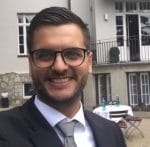 Speaker: Stefan Bauer
is Application Engineer at Siemens EDA to support the European Distribution Channel in the digital design and verification area.
Before he joined Siemens EDA in 2014, he worked as a Verification Engineer at Ericsson and ST-Ericsson in Nuremberg where he verified components of an ASIC by using SystemVerilog OVM/UVM environments, Assertions and Code Coverage.
During his job as a working student and during his master thesis at Siemens Healthcare in Erlangen, he gathered his first experiences in the FPGA area.
Portable Stimulus for SystemVerilog UVM, VHDL UVVM and C-based Verification Environments
The Portable Test and Stimulus Standard (PSS) defines a specification to create abstract, easily-reusable representations of stimulus and test scenarios. When using PSS, a single description of the verification intent is defined and the tool generates reusable scenario-level stimuli retarget-able across simulation, emulation, and other verification targets. Using PSS creates higher quality tests, controls repetition and redundancy, and results in 10X faster achievement of target coverage.
This new standard will be introduced and shown how PSS can be used to generate scenario-level tests for SystemVerilog UVM, VHDL UVVM, and even C-based verification environments from a single abstract model.
 Speaker: Stefan Bauer
is Application Engineer at Siemens EDA to support the European Distribution Channel in the digital design and verification area.
Before he joined Siemens EDA in 2014, he worked as a Verification Engineer at Ericsson and ST-Ericsson in Nuremberg where he verified components of an ASIC by using SystemVerilog OVM/UVM environments, Assertions and Code Coverage.
During his job as a working student and during his master thesis at Siemens Healthcare in Erlangen, he gathered his first experiences in the FPGA area.
Requirement Management for the development of safety crictical applications
With increasing complexity of electronic components in the safety critical domain a systematic approach of development planning and analysis of its progress during the life cycle of the application becomes more and more important. Application Life Cycle Management (ALM) is the buzzword that refers to the automation of processes in the application’s life cycle. As a central part of this ALM process, the product requirements need to be clearly traceable, from the creation through all development activities down to the results of verification, validation and test. This requirement tracking is the key for successful audits, to get the safety critical application certified for usage in the target product, which could be a medical, an automotive, an aerospace or railway application.
The presentation will provide an overview of the possibilities to manage requirements in Polarion®, including the possible integration into the FPGA design and verification process.
 Speaker: Hans-Jürgen Schwender
has a masters degree in electrical engineering. From 1991 until the end of 2001, he worked as an ASIC design engineer at Philips Kommunikationsindustrie and Lucent Technologies in Nuremberg and at Infineon Technologies in San Jose, CA, USA. He worked on the creation of specifications, the implementation in VHDL, verification on module and chip level as well as programming of ASIC Driver Software in C.
Mr. Schwender has been working at TRIAS Mikroelektronik since 2002 and, as the technical manager covers a large part of Siemens EDA’s products – with a focus on HDL design, verification and cable harness design products.
Getting your FPGA certified – according to functional safety standards
Functional safety is becoming ever more important and there are several standards in place which define how it is categorised and measured. If your customer requires compliance with one or more of these standards you will need to understand the various levels of functional safety and how they are measured. In this presentation we examine how functional safety is defined, how it is measured, and what steps you need to take to achieve certified compliance.
 Speaker: Nigel Woolaway
received his bachelor’s degree in communications engineering from the University of Kent in 1981. He first became involved in EDA while at Standard Telephones and Cables in 1983, before moving to STMicroelectronics. He joined Siemens EDA in 1992 as technical leader of the ASIC Vendor Program in Europe. In 1995 he took on a similar role in Synopsys where he managed the European Semiconductor Vendor Program until 2004. Since 2005 he is the Co-President of Leading Edge, specialising in the introduction of new tools and methodologies to the EDA marketplace
Optimization of FPGA timing and performance with AI
Das Erreichen von Timingvorgaben von FPGA Designs kann eine sehr komplexe Aufgabe sein. Die Ergebnisse hängen von sehr vielen Parametern ab, die die Synthese und insbesondere auch Place and Route Ergebnisse beeinflussen. Die Kunst ist, die richtigen Einstellungen aller Parameter zu finden, um das optimale Timingergebnis zu bekommen. Bei einer so großen Zahl von Parametern, die den Place and Route Vorgang steuern, ist ein händischer Ansatz nicht zielführend.
Plunify haben mit ihrer Lösung InTime ein Hilfsmittel geschaffen, dass die Timingresultate analysiert und basierend auf in der Vergangenheit erzielten Timingergebnissen neue Einstellungen wählt, um so das Timing weiter zu verbessern und auch die Ausführung von vielen Synthese- und P&R Läufen parallel ermöglicht, um so Zeit zu gewinnen.
Der Vortrag stellt die Lösung InTime von Plunify vor und zeigt, welche Möglichkeiten zur automatisierten Timingoptimierung für FPGA Designs bestehen.
 Sprecher: Hans-Jürgen Schwender
ist Dipl.-Ing. Elektrotechnik und hat von 1991 bis Ende 2001 bei Philips Kommunikationsindustrie AG bzw. Lucent Technologies in Nürnberg und bei Infineon Technologies in San Jose, CA, USA, als ASIC Design Ingenieur gearbeitet. Er beschäftigte sich mit dem Erstellen von Spezifikationen, der Implementierung in VHDL, der Verifikation auf Modul- und
Chipebene als auch mit Programmierung von ASIC Driver Software in C.
Seit 2002 arbeitet er bei TRIAS Mikroelektronik GmbH in Krefeld als Technischer Leiter und deckt einen Großteil der Produkte von Siemens EDA ab – mit Schwerpunkt HDL Design, Verifikation und Kabelbaumentwurfsprodukte.
Extreme visibility into the FPGA: the way to better design, verify, debug… and monitor
In den letzten Jahren haben FPGA Anbieter den FPGA DesignFlow revolutioniert und neue Architekturen eingeführt, während gleichzeitig die Anforderungen traditioneller und neuer FPGA Anwendungen berücksichtigt wurden. Gleichzeitig hat die Komplexität von FPGAs ein beispielloses Ausmaß erreicht, wodurch die üblichen EDA und Instrumentierungs Tools manchmal weniger relevant oder völlig überholt sind. In dieser Präsentation konzentrieren wir uns auf die Sichtbarkeit des FPGA als Schlüsselmerkmal für die Verbesserung von Design, Überprüfung, Debug und sogar der Überwachung von FPGAs im Einsatz.
 Sprecher: Frédéric Leens
ist der CEO und Gründer von Exostiv Labs. Vor dem Start von Exostiv Labs in 2015 war Frederic CEO von Byte Paradigm, einer Firma, die er 2005 gründete, um Unternehmen Instrumentierungsprodukte auf PC-Basis Board-Level bereitzustellen. Zuvor war er Projektleiter und Systemarchitekt bei Barco, dem Spezialisten für Display- und Visualisierungstechnologien. Er leitete erfolgreich Kontinent übergreifende Teams für Projekte im Bereich Elektronik, die Siliziumchip- und Software-Design umfassten.
Frédéric verfügt über eine 20-jährige Berufserfahrung in Branchen, die von Halbleitern über Bildverarbeitung und Medienübertragung bis hin zu Luftfahrt und Telekommunikation reichen.
Random HW Fault Analysis
Standards für funktionale Sicherheit (z.B. ISO 26262 oder DO-254) fokussieren sich auf zwei Bereiche von möglichen Fehlern: Systematische Fehler und zufällig auftretende Hardware Fehler.
Die systematische Fehleranalyse stellt sicher, dass das Design einwandfrei nach den Vorgaben der Spezifikation funktioniert. Systematische Fehler können z.B. durch unvollständige oder falsch interpretierte Spezifikation oder durch fehlerhaften Designcode auftreten und sie können durch den traditionellen Design- und Verifikationsansatzes gefunden und behoben werden.
Zufällig auftretende Fehler sind hardwarespezifisch. Jedes elektronische Gerät ist Störeinflüssen von außen, wie z.B. elektromagnetische Störungen, ausgesetzt. Falls aufgrund von solchen Störeinflüssen ein Fehler auftritt, dann muss die Hardware entweder in einen vordefinierten Sicherheitszustand schalten oder weiterhin sicher arbeiten.
Aber wie kann man solche zufällig auftretenden Hardware Fehler verifizieren?
In diesem Vortrag wird Siemens EDAs einzigartige Lösung für die Analyse von zufällig auftretenden Hardware Fehlern vorgestellt.
 Sprecher: Stefan Bauer
ist Applikationsingenieur bei Siemens EDA und unterstützt den europäischen Distributionskanal im digitalen Design- und Verifikations-Bereich.
Bevor er 2014 zu Siemens EDA nach München kam, verifizierte er als Verifikationsingenieur bei Ericsson und ST-Ericsson in Nürnberg Komponenten eines ASICs. Hierbei wurden neben der Verifikationssprache SystemVerilog und der Methodik OVM/UVM auch Assertions und Code Coverage eingesetzt.
Seine ersten Erfahrungen im FPGA Bereich sammelte er bei seinem Werkstudentenjob und bei seiner Diplomarbeit bei Siemens Healthcare in Erlangen.
Portable Stimulus for SystemVerilog UVM, VHDL UVVM and C-based Verification Environments
Der Portable Test and Stimulus Standard (PSS) definiert eine Spezifikation, um abstrakte und einfach wiederverwendbare Darstellungen von Stimulus- und Testszenarien zu erstellen. Bei der Verwendung von PSS wird eine einzige Beschreibung der Verifikationsabsicht definiert und das Tool generiert wiederverwendbare Stimuli auf Szenarioebene, die in Simulation, Emulation und anderen Verifikationsbereichen verwendet werden können. Durch die Verwendung von PSS werden Tests mit höherer Qualität erstellt, Wiederholungen und Redundanzen kontrolliert und die Testabdeckung um das Zehnfache schneller erreicht.
Dieser neue Standard wird vorgestellt und es wird gezeigt, wie PSS ausgehend von einem einzelnen abstrakten Modell bei Tests auf Systemebene für SystemVerilog / UVM-, VHDL- und sogar C-basierte Verifikationsumgebungen eingesetzt werden kann.
 Sprecher: Stefan Bauer
ist Applikationsingenieur bei Siemens EDA und unterstützt den europäischen Distributionskanal im digitalen Design- und Verifikations-Bereich.
Bevor er 2014 zu Siemens EDA nach München kam, verifizierte er als Verifikationsingenieur bei Ericsson und ST-Ericsson in Nürnberg Komponenten eines ASICs. Hierbei wurden neben der Verifikationssprache SystemVerilog und der Methodik OVM/UVM auch Assertions und Code Coverage eingesetzt.
Seine ersten Erfahrungen im FPGA Bereich sammelte er bei seinem Werkstudentenjob und bei seiner Diplomarbeit bei Siemens Healthcare in Erlangen.
Requirement Management for the development of safety crictical applications
Steigende Komplexitäten von elektronischen Geräten, deren Anwendung in sicherheitskritischen Bereichen stattfindet, erfordern eine systematische Planung des Entwicklungszyklus und die Analyse zu jeder Zeit innerhalb des Lebenszyklus einer Anwendung. Application Lifcecycle Management (ALM) ist das Stichwort, mit dem man die Automatisierung von Abläufen im Lebenszyklus der Anwendungen beschreibt. Teil dieses ALM Prozesses ist die Möglichkeit, die Produkt-Requirements innerhalb des Entstehungs- und Entwicklungsprozesses durchgängig nachvollziehbar zu machen. Dieses Requirement Tracking ermöglicht es, ein Requirement durch alle Ebenen der Dokumentation bis zur Implementierung und der Verifikation einer Produktkomponente nachzuverfolgen, so dass die Zertifizierung des Produktes für eine Anwendung in Bereichen wie Medizintechnik, Automobil, Luftfahrt, Bahntechnik usw. stark vereinfacht wird.
Die Präsentation gibt einen Überblick über die Möglichkeiten des Requirement Managements in Polarion® und die Möglichkeiten der Anbindung an den FPGA Entwicklungsprozess und der Verifikation.
 Sprecher: Hans-Jürgen Schwender
ist Dipl.-Ing. Elektrotechnik und hat von 1991 bis Ende 2001 bei Philips Kommunikationsindustrie AG bzw. Lucent Technologies in Nürnberg und bei Infineon Technologies in San Jose, CA, USA, als ASIC Design Ingenieur gearbeitet. Er beschäftigte sich mit dem Erstellen von Spezifikationen, der Implementierung in VHDL, der Verifikation auf Modul- und Chipebene als auch mit Programmierung von ASIC Driver Software in C.
Seit 2002 arbeitet er bei TRIAS Mikroelektronik GmbH in Krefeld als Technischer Leiter und deckt einen Großteil der Produkte von Siemens EDA ab – mit Schwerpunkt HDL Design, Verifikation und Kabelbaumentwurfsprodukte.
Getting your FPGA certified – according to functional safety standards
Funktionale Sicherheit wird immer wichtiger. Es gibt verschiedene Standards, die definieren, wie diese Sicherheit kategorisiert und gemessen wird. Wenn Ihre Kunden die Erfüllung einer oder mehrerer Normen fordern, müssen Sie die verschiedenen Ebenen der funktionalen Sicherheit kennen und wissen.
In diesem Vortrag untersuchen wir, wie funktionale Sicherheit definiert und gemessen wird und was Sie unternehmen müssen, um Ihr Zertifikat zu erhalten.
 Sprecher: Nigel Woolaway
erwarb 1981 seinen Bachelor der Nachrichtentechnik an der University of Kent. Die erste Mitwirkung an EDA hatte er bei Standard Telephones and Cables im Jahr 1983, bevor er zu STMicroelectronics wechselte. Er kam 1992 als technischer Leiter des ASIC Vendor Program in Europa zu Siemens EDA. 1995 übernahm er eine ähnliche Rolle bei Synopsys, wo er bis 2004 das European Semiconductor Vendor Program leitete. Seit 2005 ist er Vizepräsident von Leading Edge und ist spezialisiert auf die Einführung neuer Tools und Methoden auf dem EDA-Markt.

